A GaN charger is a power adapter built around gallium nitride transistors instead of silicon ones, which lets an adapter of a given wattage be smaller and lose less energy as heat.
The material is only one part of the story, and this page sits inside the wider gadget buying guide to help separate what the semiconductor changes from what it leaves alone.
Gallium nitride in brief
Gallium nitride, usually written GaN, is a compound of gallium and nitrogen. Reference sources describe it as a binary semiconductor with a wide band gap of 3.4 eV. The band gap is the energy a charge carrier needs to jump into the conducting state, and a wide one makes a material more resistant to the effects of heat and high voltage. GaN is not new technology: it has been commonly used in blue light-emitting diodes since the 1990s, long before it reached the power adapters that plug into a wall.
What changed more recently is the manufacturing of transistors made from the material at a cost low enough for consumer products. According to the same reference, GaN power transistors have come into increasing use in power supplies since the early 2020s, where they convert AC mains electricity to low-voltage DC.
Wide band gap, smaller adapters
Every phone or laptop adapter performs the same basic job. It takes alternating current from a wall socket and, through a rapidly switching circuit, turns it into the low-voltage direct current a device needs. The switching transistors are the part where most of the design effort goes, because each switching event wastes a little energy as heat, and that heat must be managed by the size of the components and the case around them.
Here GaN has three practical advantages over silicon, all traceable to the wide band gap. First, the performance of GaN transistors is maintained up to higher temperatures, about 400 °C against about 150 °C for silicon transistors, according to the reference. Second, GaN is efficient at transferring current, which means less energy is lost to heat. Third, GaN power transistors are valued for their small size and fast switching speed. Faster switching generally allows the magnetic parts of a converter, such as the transformer, to be smaller, and that is where much of the visible shrinkage in an adapter comes from.
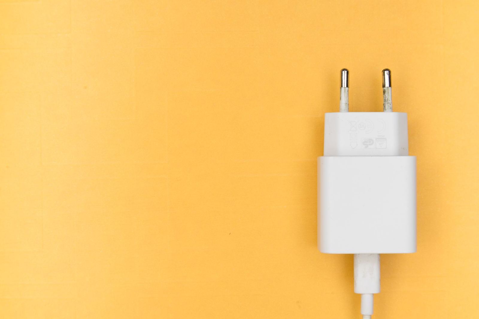
The reference sums up the effect by noting that the higher efficiency and high power density of integrated GaN power management ICs allows them to reduce the size, weight and component count of applications including mobile and laptop chargers. Its illustration compares a 30 W GaN USB-PD wall charger with a traditional silicon-based charger of the same power rating and describes the GaN unit as significantly smaller.
- GaN in blue LEDs since 1990s: 1990s
- GaN less energy lost to heat: less energy lost to heat
- Use in power supplies since early 2020s: early 2020s
- GaN ICs reduce size, weight and component count of chargers: size, weight, component count
The limits of the material
A GaN adapter still follows the same rules as any other adapter on the receiving side. The wattage a phone or laptop actually receives is decided by a negotiation between charger and device, not by the semiconductor inside the charger. For USB-C chargers, that negotiation is described in the guide to usb-c power delivery. In that scheme, devices request a level of electrical power through a bidirectional data channel, up to 5 A and 20 V in the standard profiles, and the charger offers what it supports.
The standard itself has grown over time. The reference lists the first modern Power Delivery specification in 2012 at up to 60 watts, version 2.0 in 2013 at up to 100 W, and USB PD 3.1 in 2021, which raised the maximum to 240 W. The same reference cites the USB Implementers Forum specification, which describes the top tier as Extended Power Range, a framework for power delivery up to 240W (48V at 5A) over certified USB Type-C interfaces. A GaN charger is one way to build hardware that serves these profiles compactly; a silicon charger can serve the same profiles at a larger size, and a GaN charger can still be limited to a modest profile.
That distinction matters when comparing adapters. A GaN label on the box says something about the construction, while the profiles printed on the adapter say what it can deliver to a given device. A phone that accepts a modest wattage will not draw more because the adapter uses a newer material.
Reading the specifications
The output ratings printed on the adapter body and in the manufacturer’s documentation are the authoritative description of what it can do. Typical items to look for are the voltage and current pairs listed for each output, whether the total power is shared when more than one port is in use, and which charging standards the manufacturer says it supports. Because the rating is the manufacturer’s own statement, it is worth reading it rather than relying on the material name used in marketing.
Cables are part of the same chain. A cable that is not rated for the current a profile needs will limit the result, which is why the standard includes electronically marked cables for the higher tiers. The details are covered in the guide to USB-C power delivery linked above, and the manufacturer of a particular adapter or device is the right source for which cable it expects.
Chargers and batteries are often discussed together, since a larger adapter is often bought to refill a portable battery. How a battery’s rated capacity relates to what a device can actually draw from it is explained in the guide to power bank capacity.
Heat and efficiency claims
Efficiency claims for chargers can be confusing, because a few percentage points of difference in conversion efficiency changes the heat output without changing how fast a phone charges. The reference makes a general statement, that GaN is efficient at transferring current and so less energy is lost to heat. It does not translate that into a specific saving for every product, and individual adapters vary with their design, their power rating and the load placed on them.
The wide band gap also helps explain why designers can pack a GaN converter more tightly. Components that tolerate heat well can sit closer together, and switching faster allows smaller magnetics. These are design choices rather than guarantees, so two GaN adapters of the same wattage can still differ in size, in the number of ports and in how they share power between them.
Frequently asked questions
Does a GaN charger charge a phone faster?
Show answer
Not by itself. The charging speed is set by the profile the phone and charger negotiate, as described in the USB Power Delivery specification, and by what the phone accepts. The semiconductor affects the size and the heat of the adapter.
Is GaN a new material?
Show answer
No. Reference sources note that gallium nitride has been commonly used in blue light-emitting diodes since the 1990s. Its use in power supplies for consumer electronics is the more recent development.
Why are GaN chargers smaller?
Show answer
The material tolerates higher temperatures and switches quickly, which allows a converter to use fewer and smaller components. The reference describes a GaN adapter as significantly smaller than a silicon-based one of the same power rating.
Do all USB-C chargers support the same wattage?
Show answer
No. The Power Delivery specification defines several power levels, and each adapter supports the ones its manufacturer lists. The label on the adapter and the manufacturer’s documentation state which.